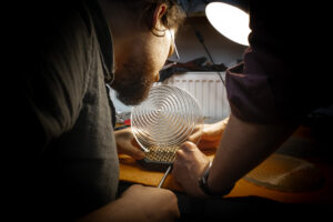
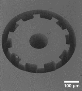
Two-photon polymerization, used in two-photon (2PP) 3D printing, is a powerful tool enabling the production of three-dimensional micro- and nanostructures of any shape. It is increasingly used in nanophotonics, micromechanics as well as microfluidics and tissue engineering.
micro-, nano- , piko-, femto-
Let’s start, however, by discussing what orders of magnitude are we talking about. The “largest” of these values – micrometer, is only 0.000001 meters. For comparison, human hair is about 50-100 microns.
However, the scale of two-photon polymerization goes even lower. One nanometer is one billionth of a meter, which is again much easier to imagine with examples: human hair has a diameter of up to 100,000 nanometers, human red blood cell is about 7,500 nanometers, and the strand of human DNA is 2.5 nanometers in diameter.
The key size for two-photon (2PP) 3D printing is femtosecond, i.e. the duration of one pulse used in this laser technique. Femto is a prefix for 10-15, so femtosecond is only 0.000000000000001 seconds. For comparison, the blink of an eye lasts 0.3 – 0.4 seconds – over 10,000,000,000,000 times longer.
Why a femtosecond laser?
Unlike standard pulse lasers and continuous-beam lasers, femtosecond lasers very quickly deliver a huge amount of energy in a very short period of time.
Femtosecond pulses (fs) supply energy to the electron subsystem in less time than electrons need to pass it to the structure – this means ultra-fast interactions between the material and the laser beam.
2PP additive technology is based on the process of two-photon absorption in the near infrared range. By combining non-linear effects, careful selection of beam parameters and laser focusing, it is possible to achieve 3D printing resolution of up to 100 nm. In addition, 2PP printing occurs in the volume of the material, not on its surface, which allows creating much more complex shapes at a much higher speed.
During the subtractive treatment using the femtosecond laser, the thermal effect is minimal, which allows the material to be processed “cold” without thermal damage to the surrounding material. Thanks to this, cutting and drilling with ultra-short pulses gives high quality and previously unattainable resolution.
Entire nanofabrication in one device
Two-photon additive production and subtractive methods – imagine the potential of a system combining both of these techniques!
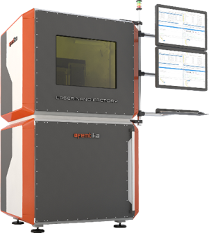
The Lithuanian company Femtika, derived from the Laser Research Center of the University of Vilnius, has developed one of the most groundbreaking systems of recent years – a hybrid system for micro- and nanofabrication Femtika Nanofactory. As they say, their main goal is to meet the growing worldwide demand for universal tools and technologies enabling the production of custom components at the micro and sub-micron scale.
The microfabrication process in this one device not only includes 2PP photopolymerization, but also uses the laser ablation process and selective laser etching (SLE; Selective Laser Etching).
Dedicated 3DPoli software allows full control of related devices (both manually and from user-defined scripts). The system is modular, it can be modified according to specific needs and requirements, e.g. attach optical fiber holders or integrate with an automatic production line.
IMPOSSIBLE BECOMES POSSIBLE
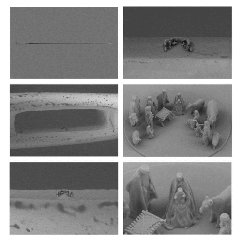
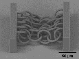
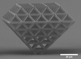
There is no other system in the world whose capabilities include the production of flexible, mobile structures at the microscale. An example is a “chain mail” (Figure 2) made of hard but flexible materials in the microscale (for example the SZGel photopolymer). The name of the SZGel photopolymer comes from the silicon (Sr) and zirconium (Zr) contained in it. Due to the high density of gels used in two-photon printing, the uncured material is in itself a support for printed elements. This provides the opportunity to create such complex structures as “chain mail” without additional supporting elements.
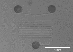
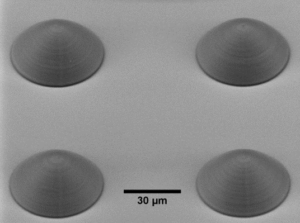
By using selective laser etching, it is possible to create all elements of the microfluidic system during one technological stage (Figure 3). Femtika Nanofactory allows the production of systems containing elements of various shapes and sizes from fused silica.
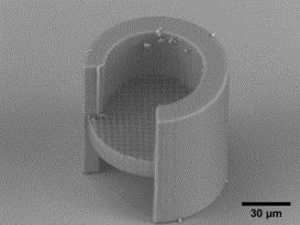
By using a very large numerical aperture of the optical system (NA up to 1.4) it is possible to produce repetitive structures with dimensions below 200 nm and periodicity below 400 nm.
The production of such small and diverse elements at the micro- and nanoscale brings the whole world of science to the next stage. Not only tissue engineering, but also nanophotonics, micromechanics and microfluidics have a huge breakthrough, Femtika Nanofactory gives us opportunities that we could only dream of before.